


News Trends
【Industry News】Gallium Oxide Comprehensive News —— International Section
日期:2024-10-24阅读:1829
1、Tohoku University Establishes New Company to Achieve Low-Cost Mass Production of Gallium Oxide Wafers
Tohoku University announced the formation of a startup company called FOX, which aims to achieve the mass production of low-cost β-type Gallium Oxide (β-Ga2O3) wafers. The precious metal-free single crystal growth technology developed by Tohoku University and C&A will be utilized to produce β-Ga2O3 bulk/substrate with a defect density comparable to Silicon at a lower cost than Silicon Carbide (SiC).
Tohoku University announced on October 17, 2024 that it will establish a startup company FOX to achieve low-cost mass production of β-Gallium Oxide (β-Ga2O3) wafer. Using the precious metal-free single crystal growth technology jointly developed by Tohoku University and C&A, the aim is to commercialize the technology to produce a β-Ga2O3/substrate with a similar defect to Silicon at a cost lower than Silicon Carbide (SiC).
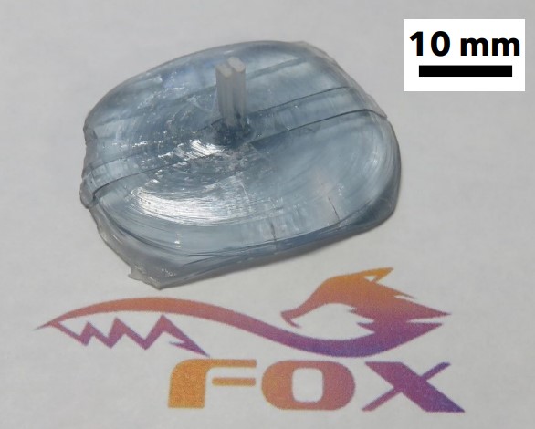 β-Ga2O3 crystal bulk grown by OCCC method. Source: Tohoku University, Japan
As a new power semiconductor material, β-Ga2O3 has a wider band gap than SiC and GaN, as well as higher performance and lower energy loss. In addition, β-Ga2O3, like Silicon, can produce a large number of high-quality single crystal at one time by growing crystals from the raw material melt solution. The growth rate is 10 to 100 times faster than SiC, and it is considered to be "the most productive among the new generation of semiconductor materials". Theoretically, the single crystal substrate with low defect can be prepared by this method at low cost.
However, conventional crystal growth methods require the use of the precious metal iridium as a crucible to accommodate the high melting point of the melt solution, and the crucible needs to be replaced regularly. The cost of iridium accounts for more than 60% of the total cost of the semiconductor front-end process (including thin film manufacturing), which greatly hinders the reduction of the cost of β-Ga2O3 device manufacturing. Currently, β-Ga2O3 substrates are more expensive than SiC, limiting the popularity of β- Ga2O3. The establishment of FOX aims to address this issue.
Achieve Low-Defect Wafers Comparable to Silicon at a Cost Lower than SiC
FOX will use the OCCC (Oxide Crystal growth from Cold Container) method to produce β-Ga2O3 bulk without a precious metal crucible. The method aims to produce β-Ga2O3 bulk/substrate with a defect density comparable to Silicon at a lower cost than SiC.
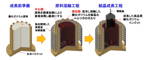
An overview of the OCCC method. Source: Tohoku University, Japan
The OCCC method was developed by Professor Akira Yoshikawa of the Institute of Metal Materials Research at Tohoku University, Associate Professor Kei Kamada of the Joint Research Center for Future Science and Technology, and a research team at C&A. In April 2022, the team announced that it had successfully developed the technology and produced β-Ga2O3 bulk single crystal.
Mass Production of 6-Inch Wafers by 2028, IPO Planned for 2033
In April 2024, FOX took over the project from Tohoku University start-up C&A and Professor Akira Yoshikawa's research group, and expects to set up a production site in the Tohoku region of Japan.
At the press conference on the 17th of this month, President Akira Onodera stressed that the cost of substrate production in the production of Gallium Oxide power semiconductors accounts for more than 60% of the total cost, and we aim to reduce this cost and promote the application and popularization of Gallium Oxide in society.
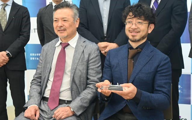
FOX President Akira Onodera (left) and Professor Akira Yoshikawa of Tohoku University (right).
Tohoku University said: "This technology is expected to break through the bottlenecks in the price and quality of Gallium Oxide and promote the social application of the next generation of Gallium Oxide power semiconductors." According to the forecast of Fuji Keizai, although the Gallium Oxide market size is only 2 billion yuan in 2030, it is expected to expand the market significantly through this technology." The company will initially focus on developing technology to produce large-size semiconductor-grade crystals using the OCCC method, accelerate technology development, and achieve mass production of 6-inch wafers by 2028. It will then expand its production capacity, advance the validation of 6-inch wafers and plan an initial public offering (IPO) in 2033.
2、Japan’s NCT Gains NEDO Funding for Project to Develop β-Ga2O3 Wafers, Power Devices and Power Modules
Novel Crystal Technology Inc (NCT) of Saitama, Japan, which develops and sells gallium oxide wafers, says that an R&D project related to beta-phase gallium oxide (β-Ga2O3) was adopted by Japan’s New Energy and Industrial Technology Development Organization (NEDO). The project ‘Development of Material Technology for High-Output and High-Efficiency Power Devices/High-Frequency Devices’ is part of the ‘Key and Advanced Technology R&D through Cross Community Collaboration Program’ (K Program) promoted by Japan’s Cabinet Office (CAO), the Ministry of Education, Culture, Sports, Science and Technology (MEXT), and the Ministry of Economy, Trade and Industry (METI).
For the project, which has a budget of ¥4.5bn and a planned duration of five years from fiscal 2024 to fiscal 2028, NCT will collaborate with related companies and academic institutions to develop β-Ga2O3 wafers, power devices, and power modules.
Specifically, NCT will work on the development of low-cost crystal growth technology for manufacturing 6-inch high-quality β-Ga2O3 wafers and 6-inch homoepitaxial growth technology with low defect density and high production throughput.
In addition, in collaboration with Tokyo-based Mitsubishi Electric Corp, NCT will work on the development of a high-voltage β-Ga2O3 transistor with high breakdown voltage of 3.3kV or more, and low on-resistance which is less than half that of silicon carbide (SiC). Mitsubishi Electric will also work on the development of a power module in which multiple β-Ga2O3 transistor chips are assembled in parallel. Nagoya-based Japan Fine Ceramics Center will work on the construction of non-destructive, high-speed full-surface defect inspection technology for 6-inch β-Ga2O3 wafers.
3、Collaboration Between The Ohio State University and Taiyo Nippon Sanso to Introduce MOCVD and HVPE for the Development of Advanced Nitride and Oxide Material Devices
Taiyo Nippon Sanso Corporation (Headquarters: Shinagawa-ku, Tokyo; President: Kenji Nagata; hereinafter “TNSC”), a Japanese industrial gas business company in the Nippon Sanso Holdings Group, and The Ohio State University announce that Ohio State will purchase and use a TNSC SR4000HT-RR-LV metal organic chemical vapor deposition (MOCVD) reactor for its advanced nitride research and development and a halide vapor phase epitaxy (HVPE) reactor for advanced gallium oxide applications.
“Taiyo Nippon Sanso is very proud to establish a relationship with The Ohio State University for research and development of gallium nitride and gallium oxide materials and devices. Taiyo Nippon Sanso is looking forward to working with Professors Steven A. Ringel, Siddharth Rajan, and Hongping Zhao and The Ohio State University community to further establish its reputation as a center of excellence in the field of wide band gap semiconductor research and development,” said TNSC Senior Corporate Officer Kunihiro Kobayashi.
“The Ohio State University is very excited to partner with Taiyo Nippon Sanso,” said Professor Steven A. Ringel, Associate Vice President of Research at The Ohio State University, and Executive Director of Ohio State’s Institute for Materials and Manufacturing Research (IMR). “The selection of the TNSC MOCVD and HVPE systems and our partnership with Taiyo Nippon Sanso enables The Ohio State University to expand its epitaxial growth facilities with these state-of-the-art growth capabilities for nitrides and oxides. We are eager to leverage TNSC technology to push the boundaries of wide and ultrawide bandgap semiconductor research and development.”
The MOCVD and HVPE reactors will be installed at Nanotech West Lab, a 36,000-square-foot shared user facility servicing the Ohio State materials community. The lab is operated by IMR, a multidisciplinary institute that provides infrastructure support and development, as well as management of major research facilities at Ohio State.
As research and applications for advanced nitride materials and devices expand, TNSC expects its MOCVD and HVPE platforms to be the platforms of choice for researchers and manufacturers.
Taiyo Nippon Sanso Corporation
Taiyo Nippon Sanso Corporation, founded in 1910, is a global supplier of industrial gases. In 1983, TNSC launched MOCVD operations alongside its conventional industrial gas operations.
