


Paper Sharing
【Member Papers】Research Progress of Ultra-Wide Band Gap Semiconductor Materials and Devices in Xidian University
日期:2024-10-24阅读:2125
Authors: HE Yunlong, LU Xiaoli, SUN Jing, ZHANG Jinfeng, ZHENG Xuefeng, MA Peijun, MA Xiaohua, HAO Yue
(National Engineering Research Center for Wide Band-Gap Semiconductor, Xidian University, Xi 'an 710071, China)
Abstract
The ultra-wide band gap semiconductor represented by Gallium Oxide, Diamond and Aluminum Nitride is the fourth generation of semiconductor materials after Silicon, Gallium Arsenide, Gallium Nitride, and Silicon Carbide. It has been recognized as the key technology to promote the rapid development of microelectronics technology, and has become the technical commanding height of competition around the world. The ultra-wide band gap semiconductor has the advantages of high power, high voltage resistance, high temperature resistance and strong radiation resistance. It is the ideal material for the new generation of high-power integrated circuits, power electronic power devices, short-wavelength optoelectronic devices and detection devices. In this paper, we summarize the research progress of Gallium Oxide, Diamond and Aluminum Nitride semiconductor materials and devices, and look forward to the future.
Introduction
The third generation of wide band gap semiconductors, represented by Gallium Nitride and Silicon Carbide, have been widely used in the fields of radio frequency electronics, power electronics and optoelectronics, but there are still some problems to be solved. For example, the size of Gallium Nitride (GaN) single crystal substrate is small, the dynamic characteristics of the device are poor, and defect interface mechanism is not clear. Silicon Carbide (SiC) still has some technical difficulties such as high material cost and high processing difficulty. With the rapid rise of new energy and photovoltaic industry, the circuit system with large output power and low energy loss has become the future development trend, while GaN and SiC are slightly tired. Therefore, the development of ultra-wide band gap semiconductors represented by Gallium Oxide (Ga2O3), Diamond and Aluminum Nitride (AlN) has received extensive attention from industry and academia, and certain progress has been made.
The ultra-wide band gap semiconductor has a higher Bandgap than GaN and SiC, so it has a higher breakdown electric field, which can ensure that the device has a greater power density, and has superior performance such as high efficiency, high temperature resistance and strong radiation resistance. It is the ideal material for the new generation of high-power integrated circuits, power electronic power devices, short-wavelength optoelectronic devices and detection devices. The BFOM is an important indicator to judge the potential of power devices in high power applications. As shown in Figure 1, the BFOM of Gallium Oxide, Diamond and Aluminum Nitride are 4 times, 29 times and 22 times of GaN materials, respectively, and 10 times, 74 times and 56 times of SiC materials. The results show that ultra-wide band gap semiconductors have great application potential in power electronics and RF power fields. In recent years, a series of breakthroughs have been made in both material growth and device fabrication.
Combined with the latest research progress domestic and international, this paper summarizes the relevant research on Gallium Oxide, Diamond and Aluminum Nitride three ultra-wide band gap semiconductor materials and devices, and gives the future development trend, hoping to provide valuable reference information for researchers in this field.
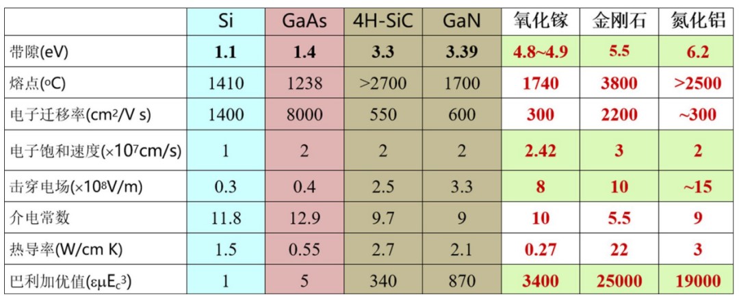
△ Figure 1. Physical properties of semiconductor materials
1.Research Progress of Gallium Oxide Materials and Devices
1.1 Gallium Oxide Materials
Ga2O3 material has an ultra-wide Bandgap (about 4.8~4.9 eV) and ultra-high critical breakdown field strength (about 8 MV/cm). Ga2O3 has five isomers, and β-Ga2O3 is the most thermodynamically stable phase at atmospheric pressure, while the other phase belong to metastable phase, and can be transformed into β- Ga2O3 under certain temperature and humidity conditions. Therefore, the current mainstream research focuses on β- Ga2O3. Compared with GaN-based devices and SiC-based devices, β-Ga2O3-based devices theoretically have lower on-resistance and lower power consumption under the same withstand voltage condition, which can greatly reduce the power loss during device operation, so β- Ga2O3 has great potential in high-power applications. At present, NCT Company in Japan has successfully prepared 6-inch (100) plane single crystal substrate by VB method, and GAREN SEMI has also achieved the growth of 6-inch single crystal substrate by casting method. Thus, the single crystal substrate of Gallium Oxide has an inherent advantage in price and cost.
The main growth methods of β-Ga2O3 include Hydride Vapor Phase Epitaxy (HVPE), Metal-organic Chemical Vapor Deposition (MOCVD) and Molecular Beam Epitaxy (MBE). Among them, HVPE has the advantages of fast growth rate and adjustable low concentration doping, which in the current market share is high. The MOCVD epitaxy growth method can not only carry out large-size epitaxy, but also take into account the growth rate, which will become the main force in the future market of Gallium Oxide epitaxy materials. At present, the β-Ga2O3 epitaxy process can be divided into homoepitaxy and heteroepitaxy. Homoepitaxy is divided into four crystal orientations: (100),(010),(001),(-201), etc. Heteroepitaxy substrates are mostly sapphire, and its main application directions are photoelectric detection, radiation detection, etc. Researchers have done a lot of work in homoepitaxy, and have made some progress. Taking (-201) plane as an example, in 2020, Jilin University prepared high-quality β-Ga2O3 homogeneous epitaxial film by MOCVD. The FWHM of its XRD rocking curves is 21.6 arcsec, and the root-mean-square (RMS) roughness is as low as 0.68 nm[1]. In 2024, Xidian University adopted pulse IN assisted technology to obtain high-quality epitaxial films with surface roughness of 0.98 nm and FWHM of rocking curve of 30.42 arcsec, as shown in FIG. 2 (a).[2] In terms of heteroepitaxy technology, XIdian University used pulse IN assisted technology to achieve high-quality heteroepitaxial films on sapphire substrate in 2023.The FWHM of the (-201) plane is 2700 arcsec, and the surface roughness is 5.1 nm[3]. In 2024, the Institute of Institute of Semiconductors, Chinese Academy of Sciences adopted a two-step method to achieve an epitaxial film with a FWHM of rocking curve as low as 0.66° and a surface roughness of 6.8 nm on a sapphire substrate, and then prepared a photodetector with a photodark current ratio of up to 1015 Jones[4], as shown in FIG. 2 (b).
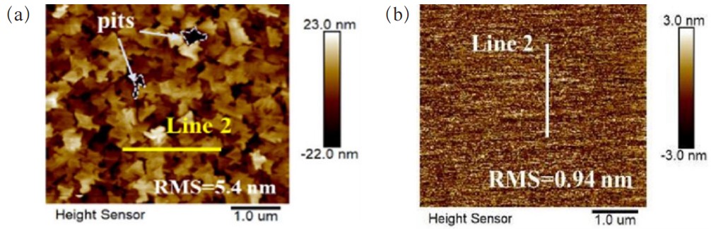
△ Figure 2. Schematic diagram of film roughness measured by AFM (a) (-201) β-Ga2O3 homogeneous epitaxial film, (b) Ga2O3 film on sapphire substrate
1.2 Gallium Oxide Devices
1.2.1 Gallium Oxide Diode
Due to the current material structure, Gallium Oxide power diodes are mainly vertical devices, and their research focuses on increasing the BFOM value of the devices, so as to approach the theoretical limit of the material. On the other hand, researchers have also done some work to reduce the turn-on voltage of Gallium Oxide power diodes to reduce the conduction loss. In order to achieve a higher BFOM value to close to the theoretical limit of its material, in 2024, the University of Florida adopted the double-layer edge dielectric terminal technology to achieve a power diode with a BFOM value of 15.2 GW/cm2, whose BFOM value is the highest[5] reported result. As early as 2022, Xidian University manufactured a composite terminal structure diode with double-layer concentration of NiOx, achieving a BFOM value of 13.2GW/cm2, with a breakdown field strength of 6.4 MV/cm and a on-resistance of 5.24 mΩ·cm2[6], as shown in Figure 3 (a).
In order to achieve a lower turn-on voltage, in 2023, the US Air Force Research Laboratory produced a vertical Pt/TiO2/ β-Ga2O3 Metal-Dielectric Semiconductor (MDS) diode, which achieved an turn-on voltage of 0.59V due to the polarization effect.[7] In the same year, Xidian University innovated the development of N2O plasma technology to treat the anode region and reduce the turn-on voltage of the diode to 0.6V[8] by forming a Ga-N bond, as shown in Figure 3 (b).
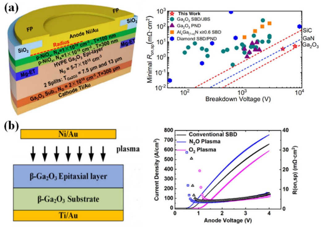
△ Figure 3. (a) Heterojunction diode of composite terminal and benchmark diagram, (b) N2O plasma treated diode and IV curve
In addition, the Gallium Oxide diode has become the most potential power device for industrialization at present, and has gradually become the focus of research. In 2022, Japan NCT company, combined with Field Plate technology, produced a high current diode with side length of 1.7 mm on a drift layer of 12 μm. The forward current of the device reached 2A@2V, the on-resistance was 17.1 mΩ·cm2, the reverse breakdown voltage was 1200 V, and the BFOM value was 84 MW/cm2[9]. In the same year, Xidian University designed a kind of hetero-junction terminal diode, the diameter is 620 μm, the forward current reaches 7.13 A@4.9 V, the on-resistance is 6.76 mΩ·cm2, the reverse breakdown voltage is 1260 V, and the BFOM value is 234 MW/cm2[10].
1.2.2 Gallium Oxide Transistor
In the field of Gallium Oxide transistors, researchers have explored a number of key issues in depth and extensively, the main research point is still focused on increasing the BFOM value of the device to close to its theoretical limit of materials, and secondly, in order to achieve future system-level applications, the realization of enhanced devices can not be ignored.
In terms of improving the BFOM value of the device, in 2022, The University of Utah produced a FIN-shaped three-channel β-Ga2O3 MESFET, which has a on-resistance of 5.1 mΩ·cm2 and a BFOM value of 0.95 GW/cm2[11]. In the same year, Xidian University produced a recessed PN heterojunction gate structure transistor, which has a on-resistance of 6.24mΩ ·cm2 and a BFOM value of 0.74GW /cm2, reaching the international advanced level. [12]
For the consideration of system application, it is very important to develop the enhanced Ga2O3-based transistor with high performance. At present, the main ways of making enhanced devices include recessed gate, heterojunction gate and Fin gate structure. In 2018, the Air Force Research Laboratory used the recessed gate structure and Atomic Layer Deposition (ALD) SiO2 as the gate medium to achieve an enhanced device with a threshold voltage of 2V, an on-resistance of 215Ω·mm, and a breakdown voltage of 505 V[13]. In 2022, the team from the University of Electronic Science and Technology of China used the recessed heterojunction gate structure to realize the enhanced Ga2O3 transistor, which has a on-resistance of 15.1 mΩ·cm2, a breakdown voltage of 980 V, and a BFOM of 63 MW/cm2[14]. In 2023, Xidian University produced Ga2O3/NiOx heterojunction gate and Schottky composite gate transistor with threshold voltage of 3.3V, breakdown voltage of 2160V, on-resistance of 6.35mΩ ·cm2, BFOM value of 0.73GW /cm2, which is the highest value reported among Gallium Oxide enhanced devices. [15] As shown in Figure 4.
In addition, due to the high critical breakdown field strength and low series resistance, Gallium Oxide still has considerable Johnson's Figure of Merit (JFOM), so it also has certain application prospects in the field of radio frequency power. Many scholars have begun to develop Gallium Oxide radio frequency transistors. In 2021, the University at Buffalo developed an enhanced (AlxGa1-x)2O3/Ga2O3 heterostructure transistor, the device’s fT, fMAX are 30, 37GHz, fT·LG reached 4.8 GHz·μm[16]. In 2023, Xidian University transferred the Ga2O3 channel material to the SiC substrate, and combined with the T-gate structure to produce the transistor, the device’s fT, fMAX are 27.6、 57 GHz, fT·LG is 5 GHz·μm, which is the highest value reported by the international, as shown in Figure 4.[17]
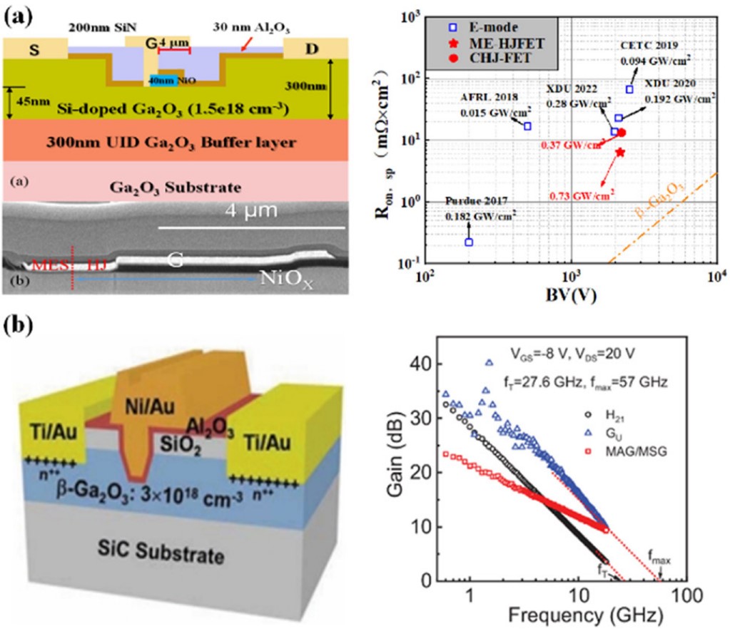
△ Figure 4. (a) Heterojunction - Schottky composite gate structure transistor and its benchmark diagram, (b) T-gate structure of β-Ga2O3 MOSFET and its small signal characteristic curve
1.Research Progress of Diamond Materials and Devices
2.1 Diamond Materials
Diamond has the advantages of large Bandgap, high breakdown field strength, high carrier mobility and high saturation velocity, and has the highest thermal conductivity in nature. From the perspective of various Figure-of-Merit of semiconductors, Diamond materials have huge application potential and are expected to push electronic components to new power limits. At the same time, Diamond also has super anti-irradiation ability, excellent electrical insulation characteristics and fast response characteristics, is expected to become the ideal material for the next generation of pulsed intense radiation field detector. In addition, Diamond can also be used as a high-performance heat sink substrate, which promotes the miniaturization of high-power devices and chips from the level of chip-level heat dissipation, and has important application value in improving the performance and life of circuits and systems.
At present, the main methods for the preparation of single crystal Diamond are High Pressure High Temperature (HPHT) synthesis and Chemical Vapor Deposition (CVD). HPHT synthesis of single crystal Diamond is a kind of technology that simulates the formation conditions of Diamond in nature, which plays an important role in scientific research and industrial applications. In 2015, Jilin University designed a new type of cubic high-pressure equipment to improve the quality of synthetic Diamond, as shown in Figure 5. [18] However, the size of single-crystal Diamond prepared by HPHT method is severely limited and cannot be further broken through.
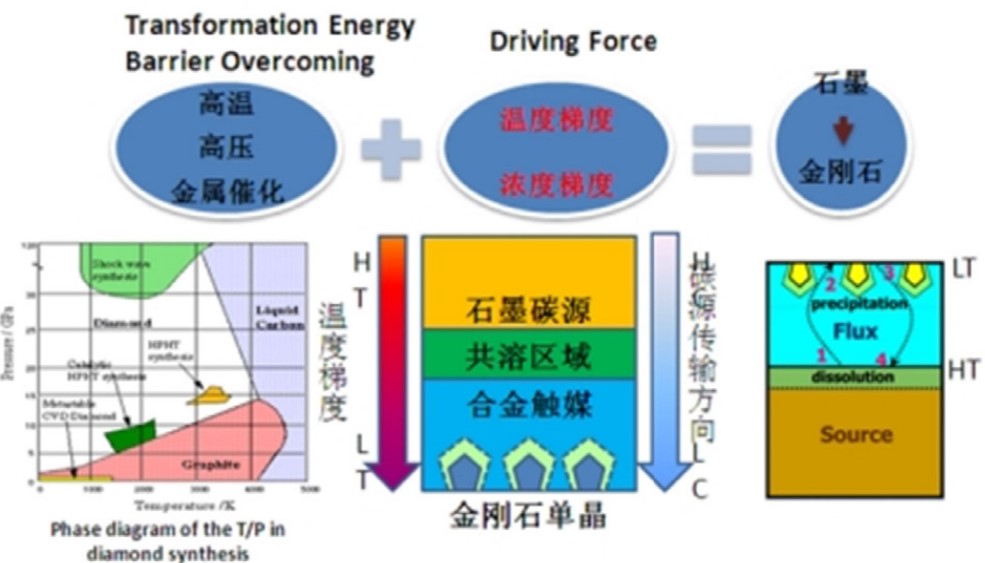
△ Figure 5. Synthesis of single crystal Diamond by HPHT.
The main methods of CVD to prepare single crystal Diamond materials or films include Microwave Plasma Chemical Vapor Deposition (MPCVD) and Hot Filament Chemical Vapor Deposition (HFCVD). After more than 40 years of development, MPCVD technology has gradually become mature and stable, and has become the mainstream way to prepare Diamond films. In 2014, Japan AIST used mosaic splicing technology to splice 24 10 mm×10 mm "clone" substrates into a 5.08 cm mosaic wafer to achieve inch-level single crystal Diamond [19]. In 2018, Xidian University used the MPCVD system to obtain a homogeneous epitaxial single crystal with a width of about 10 mm on both sides, based on the maximum edge-to-edge width of 7.5 mm of seed crystal [20]. In 2019, XIdian University used the MPCVD system to achieve simultaneous expanded growth of 7 SCD samples, and further expanded to 14 SCD samples simultaneously [21].
In terms of epitaxial growth research, in 2015, the University of Science and Technology Beijing carried out research on heteroepitaxial nucleation on Ir substrates, and the epitaxial nucleation density reached 108 ~ 109cm-2[22]. At present, the largest size (diameter ~90 mm) single crystal was obtained on Ir YSZ /Si (001) composite substrate by the University of Augsburg in 2017, with a growth time of 120 h, a thickness of 1.6 mm, and a FWHM of rocking curve (004) reaching 0.064°[23]. Xidian University optimized the MPCVD growth mode in 2020 to achieve the growth of high-purity epitaxial materials. The FWHM of the XRD (004) plane rocking curve of the material is only 46.3 arcsec[24].
2.2 Diamond Devices
2.2.1 Diamond Power Devices
Diamond power devices are divided into power diodes and power transistors. In terms of power diodes, Diamond Schottky diode is mainly realized by Schottky junction formed by P-type Diamond and metal because N-type doping technology of Diamond is not mature yet. The structure can be divided into vertical type, quasi-vertical type and horizontal type. In 2021, the National Institute of Advanced Industrial Science and Technology prepared a quasi-vertical Schottky Barrier Diode by inserting a buffer layer containing metal tungsten. At ±8 V, the rectification ratio exceeds 8 orders of magnitude, and the device breakdown voltage is 375 V[25].
Because of the inherent properties of the material, Diamond power transistors are usually depletion type devices. In 2022, the MOSFET with Al2O3 as dielectric layer was prepared by Saga University. The device maximum drain current density can reach -0.68A /mm, the maximum effective mobility is 205 cm2/ (V·s), the specific on-resistance is 7.54 mΩ·cm.2 The breakdown voltage of the device reaches 2568 V, and the BFOM value is 874.6 MW·cm,-2 which is the highest value of the Diamond power transistor at present.[26] However, more technical problems need to be overcome in order to realize enhanced devices, which is also a hot spot in the current research of Diamond power transistors. The main realization methods of Diamond enhanced devices include annealing or UV ozone treatment; using low work function gate materials; depleting 2DHG channels; nitrogen ion implantation, etc. In 2022, Xidian University used Al/BaF2 gate material to achieve high performance normally-off hydrogenated Diamond MIS-FET, the threshold voltage of the device is -0.90V, the maximum transconductance and maximum saturation current are 30 mS/mm and -96.5 mA/mm[27], respectively. In 2023, Xi 'an Jiaotong University used electron beam evaporation to deposit 30nm thick CeB6 under the gate, and successfully realized a Diamond enhanced device with a threshold voltage of -0.46V. The maximum current density is -83.8 mA/mm[28].
2.2.2 Diamond Radiation Detector
Because of its excellent anti-radiation properties and temperature stability, Diamond has a good application prospect in the field of radiation detection. The main structure of diamond radiation detector is the homogeneous mass conductivity type (junction-free type). This structure puts forward extremely high requirements for the collection characteristics of Diamond carriers produced after nuclear radiation. In terms of electrical characteristics, it is manifested as good carrier transport characteristics, few recombination centers and traps, and long recombination life of carriers. These characteristics determine the charge collection efficiency, energy resolution and the stability of long-term detection performance of Diamond radiation detectors. At present, the charge collection efficiency of Diamond radiation detector can reach more than 90% (or even 100%), and the best results for the energy resolution of α particles and neutrons are 0.4% and 1.5%, respectively. The detection of γ rays/neutrons/protons/heavy ions further proves the anti-irradiation characteristics of Diamond. After being subjected to 1015 proton/cm2, 250 Mrad photon and 3×10¹⁵ neutron/cm2 irradiation, the detection performance of Diamond only changes slightly.
In 2020, Xidian University proposed a new type of Diamond detector, which has a very low dark current of only 7.46×10⁻ ¹³ A/mm² under the electric field of 1 V/μm. Irradiated by α particles, the CCE of the detector is electron (98.6%) and electron hole (99.01%), and the energy resolution is 1.04% and 0.76%. And the detector has a ultrafast time response of only 347.4 ps[29], as shown in Figure 6.
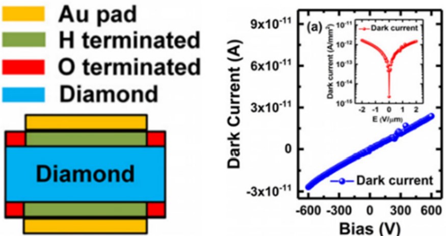
△ Figure 6. Diamond radiation detector and its IV curve
3.Research Progress of Aluminum Nitride Materials and Devices
3.1 Aluminum Nitride Materials
Aluminum Nitride (AlN) is a typical Ⅲ-V compound, with excellent physical and chemical properties such as high thermal stability (melting point 2100 ℃), high thermal conductivity [2W/(cm·K)], high chemical stability, etc. AIN also has good piezoelectric and dielectric properties, so it has great application value in energy conversion, acoustic wave and MEMS devices, and has been used in micro-electro-mechanical systems. The research on AlN materials mainly focuses on two aspects: AlN crystal growth and AlN epitaxial film. Among them, AlN crystal growth mainly adopts PVT method to grow self-seeded crystal and hetero-seeded crystal. AlN epitaxial film is mainly grown on sapphire or 4H-SiC substrate by MOCVD, ALD methods.
Many teams at domestic and international have carried out research on AlN materials and achieved certain results. In terms of AlN crystal growth, Peking University combined with effective Al atom transport control methods to achieve AlN crystals with diameters exceeding 62 mm and AlN single crystal substrates with diameters exceeding 50 mm. In terms of AlN epitaxial film, the team proposed a "controlled discrete and controlled polymerization" lateral epitaxy method (NPATs) based on a nano-patterned AlN/sapphire templates, which reduced the dislocation corrosion pit density of AlN films on sapphire substrates to the order of 104 cm-2[30]. At the same time, Xidian University proposed diffusion-adsorption-regulated epitaxy growth method to obtain a flexible AlN film of 3×3 cm2 with an RMS of 0.748 nm, as shown in Figure 7. In addition, the team continuously regulated the band gap of the flexible AlN material through strain engineering, reducing the band gap to 4.8 eV, and improved the responsiveness by 161%, the time response by 31%, and the dark current was reduced[31]. Furthermore, AlN can also be grown by ALD, acting as a gate medium. In 2015, Xidian University used PEALD to grow AlN gate medium, and combined with AlGaN/GaN to form MIS-HEMT devices. The peak of transconductance of devices is 289 mS/mm, and the gate interface characteristics are significantly improved. The interface charge is reduced to 3.1×1011cm−2[32].
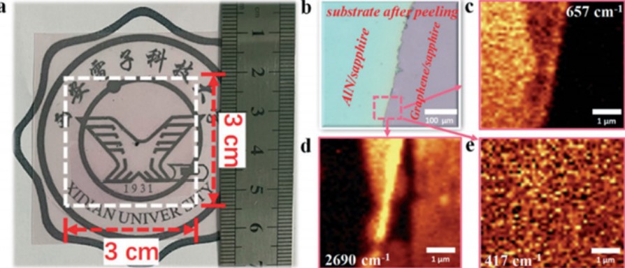
△ Figure 7. AlN thin film and its microscopic and Raman properties
3.2 Aluminum Nitride Device
Research on AlN devices mainly focuses on diodes, MESFET, photodetectors, etc. Among them, AlN-based diodes show better characteristics and have been widely studied. In 2023, Arizona State University achieved the first AlN Schottky diode on the AlN substrate with a breakdown voltage of 3 kV and a leakage current of only 200 nA[33]. In 2024, Nagoya University used distributed polarization doping method to prepare AlGaN p-n vertical diode on AlN substrate, as shown in Figure 8 (a). The breakdown field strength reached 7.3 MV/cm, the turn-on voltage of 6.5 V and the on-resistance of 3 mΩ·cm2 were realized, which is the minimum value of AlN-based p-n diode reported so far[34]. In the same year, Xidian University realized a high-performance AlN/GaN Double Barrier Resonant Tunneling Diode with a record peak current of 1551 kA/cm2 and a peak-to-valley current ratio of 1.24[35], as shown in Figure 8 (b).
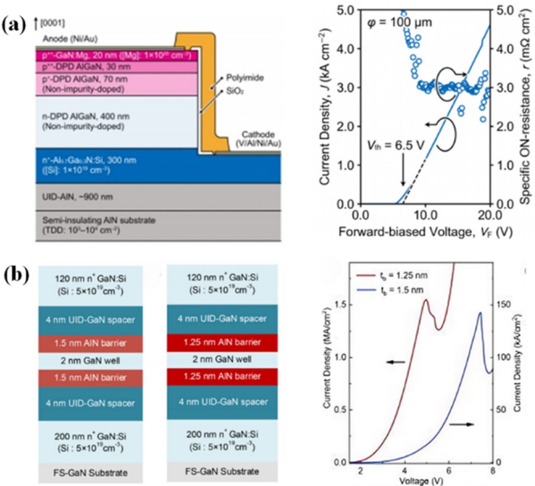
△ Figure 8. (a) Cross section of p-n diode and IV characteristic curve, (b) AlN/GaN Double Barrier Resonant Tunneling Diode and IV characteristic curve
In addition, due to the high polarization effect of AlN, the channel electron surface density in the AlN/GaN heterojunction is extremely high, which is suitable for the production of radio frequency devices, and its high ohmic contact resistance is usually solved by quadratic epitaxy. In 2022, Xidian University proposed a low-damage-enhanced AlN/GaN HEMT for remote oxygen plasma treatment, with a threshold voltage of 0.4V and a maximum current of 1.06A /mm[36]. In 2023, Peking University reported an AlN/GaN HEMT with A 70 nm gate length, ohmic contact resistance as low as 0.09 Ω·mm, fT/fmax up to 140/301 GHz, and saturation current density of 1.54 A/mm[37].
4.Summary and Prospect
This paper refers to the academic and industry trends of Ultra-Wide Bandgap Semiconductors, and briefly summarizes the key progress of Ultra-Wide Bandgap Semiconductors materials, devices and related technologies based on years of in-depth research in this field by the National Engineering Research Center.
In the “Status of the Power Electronics Industry Report”, Yole Intelligence predicts that the global power device market will grow to $33.3 billion by 2028, promoting the rapid development of the wide band gap semiconductor field. However, the existing GaN and SiC systems are difficult to meet the growing military and civilian technical requirements. As an ultra-wide band-gap semiconductor, Ga2O3 can realize the precise modulation of N-type electronic structure, Diamond has the highest thermal conductivity at room temperature, and AlN has an extremely wide band gap and better polarization characteristics. These excellent characteristics make it in the fields of high voltage, high frequency, high temperature and high-power electronic devices have broad application prospects, and it is possible to achieve low-cost and small-volume products while higher power, frequency and efficiency.
In the past decade, the world, especially the domestic research on Ultra-Wide Bandgap Semiconductors has become more active, 4-inch AlN, Diamond and 6-inch Ga2O3 substrates prepared by different technologies have been reported, Ga2O3 and Diamond MOSFET and AlN-based HEMT excellent device performance is also expected to be applied in the field of power electronics and radio frequency power. Ga2O3-based solar blind detector, Diamond-based irradiation detector and photoconductive switch, AlN-based LED and so on have also made breakthroughs in the field of optoelectronics and radiation. These promising results further prove the development potential of Ultra-Wide Bandgap Semiconductors. However, due to the immaturity of relevant theories and technologies, there are still many problems to be solved in Ultra-Wide Bandgap Semiconductors materials and devices. In addition, compared with the relatively mature SiC and GaN, the industrial application of Ultra-Wide Bandgap Semiconductors represented by Ga2O3, Diamond and AlN has just begun. In the next decade, it is believed that with the joint efforts of domestic and international counterparts, the theory and technology of Ultra-Wide Bandgap Semiconductors will be developed by leaps and bounds, and commercial products will be rapidly launched and widely used in the market. They will save energy through higher work efficiency and lower power loss, while changing people's work and life.
Extended Reading
[1] C. Zhao et al., “Preparation of high-thickness n--Ga2O3 film by MOCVD,” in Coatings, vol. 12, no. 5, 645, May. 2022, doi: 10.3390/coatings12050645.
[2] Y. Wang, et al., “Enhancing the quality of homoepitaxial (-201) β-Ga2O3 thin film by MOCVD with in situ pulsed indium,” in Applied Physics Letters, vol. 124, no. 7, 072105, Feb. 2024, doi: 10.1063/5.0189586.
[3] Y. Wang et al., “Optimization quality for indium pulse-assisted of β-Ga2O3 thin film on sapphire surface,” in Ceramics International, vol. 49, no. 23, pp. 37506-37512, Dec. 2023, doi: 10.1016/j.ceramint.2023.09.077.
[4] P. Ma et al., “Two-step growth of β-Ga2O3 on c-plane sapphire using MOCVD for solar-blind photodetector,” in Journal of Semiconductors, vol. 45, no. 2, 022502, Apr. 2024, doi: 10.1088/1674-4926/45/2/022502.
[5] J. Li et al., “Breakdown up to 13.5 kV in NiO/β-Ga2O3 vertical heterojunction rectifiers,” in ECS Journal of Solid State Science and Technology, vol. 13, no. 3, 035003, Mar. 2024, doi: 10.1149/2162-8777/ad3457.
[6] J. Zhang et al., “Ultra-wide bandgap semiconductor Ga2O3 power diodes,” in Nature Communications, vol. 13, no. 1, 3900, Jul. 2022, doi: 10.1038/s41467-022-31664-y.
[7] Nolan S. Hendricks et al., “Vertical metal-dielectric-semiconductor diode on (001) β-Ga2O3 with high-κ TiO2 interlayer exhibiting reduced turn-on voltage and leakage current and improved breakdown,” in Applied Physics Express, vol. 16, no. 7, 071002, Jul. 2023, doi: 10.35848/1882-0786/ace0f3.
[8] Y. He et al., “Research on the β-Ga2O3 Schottky barrier diodes with oxygen-containing plasma treatment,” in Applied Physics Letters, vol. 122, no. 16, 163503, Apr. 2023, doi: 10.1063/5.0145659.
[9] Q. Yan et al., “Low density of interface trap states and temperature dependence study of Ga2O3 Schottky barrier diode with p-NiOx termination,” in Applied Physics Letters, vol. 120, no. 9, 092106, Feb. 2022, doi: 10.1063/5.0082377.
[10] F. Otsuka et al., “Large-size (17x1.7 mm2) β-Ga2O3 field-plated trench MOS-type Schottky barrier diodes with 1.2 kV breakdown voltage and 109 high on/off current ratio,” in Applied Physics Express, vol. 15, no. 1, 016501, Jan. 2022, doi: 10.35848/1882-0786/ac4080.
[11] A. Bhattacharyya et al., “High-mobility tri-gate β-Ga2O3 MESFETs with a power figure of merit over 0.9 GW/cm2,” in IEEE Electron Device Letters, vol. 43, no. 10, pp. 1637-1640, Oct. 2022, doi: 10.1109/LED.2022.3196305.
[12] C. Wang et al., “Hysteresis-free and μs-switching of D/E-modes Ga2O3 hetero-junction FETs with the BV2/Ron,sp of 0.74/0.28 GW/cm2,” in Applied Physics Letters, vol. 120, no. 11, 112101, Mar. 2022, doi: 10.1063/5.0084804.
[13] K. D. Chabak et al., “Recessed-gate enhancement-mode β-Ga2O3 MOSFETs,” in IEEE Electron Device Letters, vol. 39, no. 1, pp. 67-70, Jan. 2018, doi: 10.1109/LED.2017.2779867.
[14] X. Zhou et al., “Normally-off β-Ga2O3 power heterojunction field-effect-transistor realized by p-NiO and recessed-gate,”2022 IEEE 34th International Symposium on Power Semiconductor Devices and ICs (ISPSD). Vancouver, BC, Canada, 2022, pp. 101-104, doi: 10.1109/ISPSD49238.2022.9813678.
[15] X. Wang et al., “An E-mode β-Ga2O3 metal-heterojunction composite field effect transistor with a record high P-FOM of 0.73 GW/cm2,” 2023 35th International Symposium on Power Semiconductor Devices and ICs (ISPSD), Hong Kong, 2023, pp. 390-393, doi: 10.1109/ISPSD57135.2023.10147570.
[16] A. Vaidya et al., “Enhancement mode β-(AlxGa1-x)2O3/Ga2O3 heterostructure FET (HFET) with high transconductance and cutoff frequency,” in IEEE Electron Device Letters, vol. 42, no. 10, pp. 1444-1447, Oct. 2021, doi: 10.1109/LED.2021.3104256.
[17] M. Zhou et al., “1.1 A/mm β-Ga2O3-on-SiC RF MOSFETs with 2.3 W/mm Pout and 30% PAE at 2 GHz and fT/fmax of 27.6/57 GHz,” 2023 International Electron Devices Meeting (IEDM), San Francisco, CA, USA, 2023, pp. 1-4, doi: 10.1109/IEDM45741.2023.10413782.
[18] Q. Han et al., “Design of a novel large volume cubic high pressure apparatus for raising the yield and quality of synthetic diamond,” in Journal of Crystal Growth, vol. 422, pp. 29-35, Jul. 2015, doi: 10.1016/j.jcrysgro. 2015.04.028.
[19] H. Yamada et al., “A 2-in. mosaic wafer made of a single-crystal diamond,” in Applied Physics Letters, vol. 104, no. 10, 102110, Mar. 2014, doi: 10.1063/1.4868720.
[20] Z. Ren et al., “Growth and characterization of the laterally enlarged single crystal diamond grown by microwave plasma chemical vapor deposition,” in Chinese Physics Letters, vol. 35, no. 7, 078101, Jun 2018, doi: 10.1088/0256-307X/35/7/078101.
[21] Z. Ren et al., “Multiple enlarged growth of single crystal diamond by MPCVD with PCD-rimless top surface,” in Chinese physics B, vol. 28, no. 12, 128103, Nov. 2019, doi: 10.1088/1674-1056/ab53cd.
[22] Y. Feng et al., “Heteroepitaxial nucleation of diamond on Ir(100)/MgO(100) substrate by bias enhanced microwave plasma chemical vapor deposition method,” in Journal of Synthetic Crystals, vol. 44, no. 4, pp. 896-901, Apr. 2015, doi: 10.16553/j.cnki.issn1000-985x.2015.04.009.
[23] M. Schreck et al., “Ion bombardment induced buried lateral growth: The key mechanism for the synthesis of single crystal diamond wafers,” in Scientific Reports, vol. 7, 44462, Mar. 2017, doi: 10.1038/srep44462.
[24]Su Kai. Investigation of High Performance CVD Diamond Radiation Detectors and Related Electronic Devices. Xidian University, 2022. doi: 10.27389/d.cnki.gxadu.2020.003386.
[25] P. Sittimart et al., “Enhanced in-plane uniformity and breakdown strength of diamond Schottky barrier diodes fabricated on heteroepitaxial substrates,” in Japanese Journal of Applied Physics, vol. 60, no. SB, SBBD05, May 2021, doi: 10.35848/1347-4065/abd537.
[26] N. C. Saha et al., “875-MW/cm² low-resistance NO2 p-type doped chemical mechanical planarized diamond MOSFETs,” in IEEE Electron Device Letters, vol. 43, no. 5, pp. 777-780, May 2022, doi: 10.1109/LED.2022.3164603.
[27] Q. He et al., “High mobility normally-OFF hydrogenated diamond field effect transistors with BaF2 gate insulator formed by electron beam evaporator,” in IEEE Transactions on Electron Devices, vol. 69, no. 3, pp. 1206-1210, Mar. 2022, doi: 10.1109/TED.2022.3147738.
[28] M. Zhang et al., “Electrical properties of cerium hexaboride gate hydrogen-terminated diamond field effect transistor with normally-off characteristics,” in Carbon, vol. 201, pp. 71-75, Sep. 2022, doi: 10.1016/j.carbon.2022.08.056.
[29] K. Su et al., “High performance hydrogen/oxygen terminated CVD single crystal diamond radiation detector,” in Applied Physics Letters, vol. 116, no. 9, 092104, Mar. 2020, doi: 10.1063/1.5135105.
[30] J. Wang et al., “Group-III nitride heteroepitaxial films approaching bulk-class quality,” in Nature materials, vol. 22, no. 7, pp. 853-859, Jun. 2023, doi: 10.1038/s41563-023-01573-6.
[31]Shi Zekun. Research on Polarity Control and Strain Engineering of Flexible Self Supporting AlN Thin Films. Xidian University, 2024. doi: 10.27389/d.cnki.gxadu.2022.003463.
[32] J. Zhu et al., “Improved interface and transport properties of AlGaN/GaN MIS-HEMTs with PEALD-grown AlN gate dielectric,” in IEEE Transactions on Electron device, vol. 62, no. 2, pp. 512-518, Feb. 2015, doi: 10.1109/TED.2014.2377781.
[33] D. H. Mudiyanselage et al., “High-voltage AlN Schottky barrier diodes on bulk AlN substrates by MOCVD,” in Applied Physics Express, vol 17, no. 1, 014005, 2024, doi: 10.35848/1882-0786/ad15f4.
[34] T. Kumabe et al., “Demonstration of AlGaN-on-AlN pn diodes with dopant-free distributed polarization doping,” in IEEE Transactions on Electron Devices, vol 71, no. 5, pp. 3396-3402, Feb. 2024, doi: 10.1109/TED.2024.3367314.
[35] F. Liu et al., “Record peak current density of over 1500 kA/cm2 in highly scaled AlN/GaN double-barrier resonant tunneling diodes on free-standing GaN substrates,” in Applied Physics Letters, vol 124, no. 7, 073501, Feb. 2024, doi: 10.1063/5.0180145.
[36] S. Liu et al., “Improved breakdown voltage and low damage E-mode operation of AlON/AlN/GaN HEMTs using plasma oxidation treatment,” in IEEE Electron Device Letters, vol 43, no. 10, pp. 1621-1624, Oct. 2022, doi: 10.1109/LED.2022.3203164.
[37] L. Yang et al., “AlN/GaN HEMTs with fmax exceeding 300 GHz by using Ge-doped n++ GaN Ohmic contacts,” in ACS Applied Electronic Materials, vol. 5, no. 9, pp. 4786-4791, Sep. 2023, doi: 10.1021/acsaelm.3c00555.
